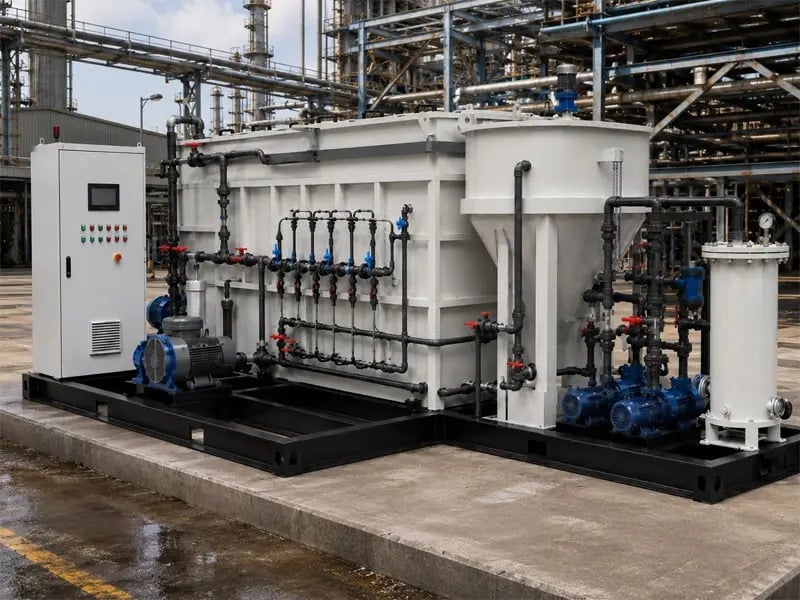
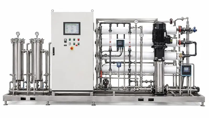
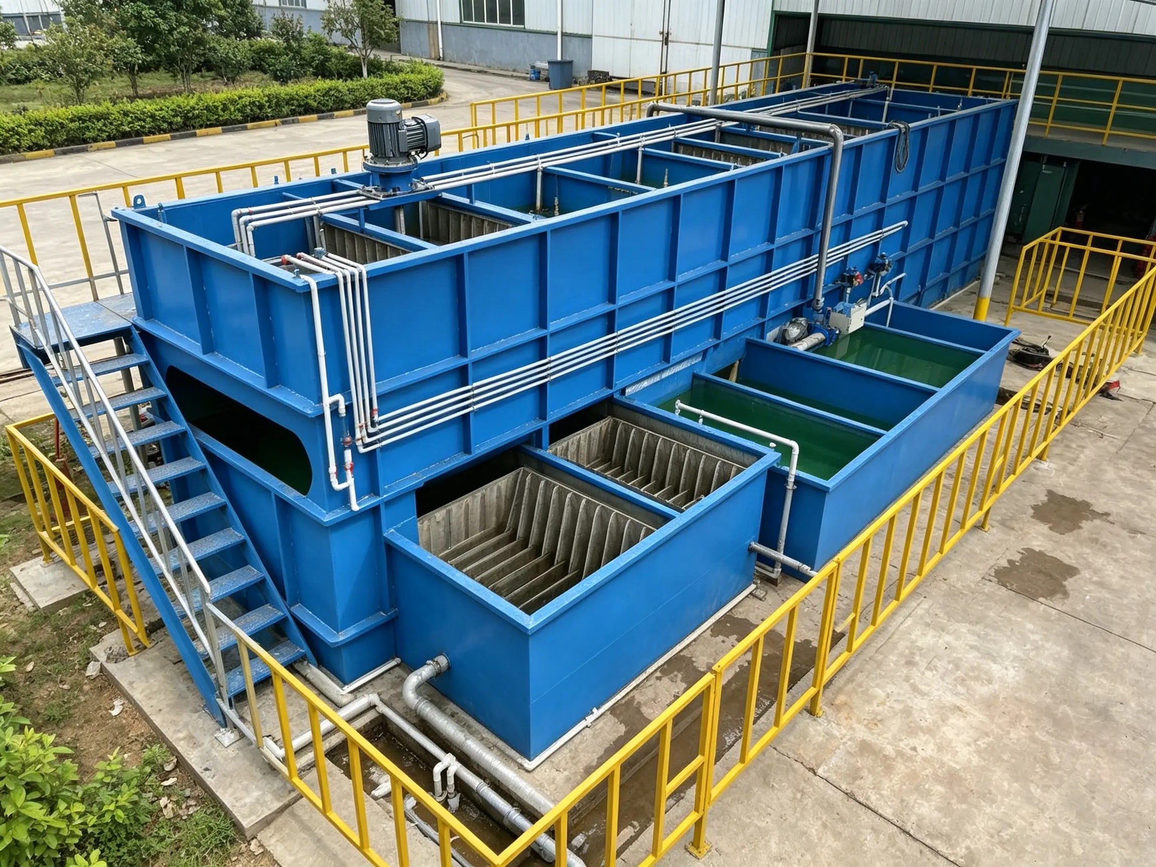
Reusing treated semiconductor wastewater represents a significant opportunity for industrial water conservation and cost reduction. However, before this reclaimed water enters manufacturing processes or cooling systems, rigorous monitoring of multiple water quality parameters is essential. The semiconductor industry generates substantial volumes of wastewater containing chemical residues, metals, and dissolved solids that require careful treatment and verification before safe reuse. Proper monitoring ensures compliance with industry standards, protects equipment, and maintains product quality throughout manufacturing operations.
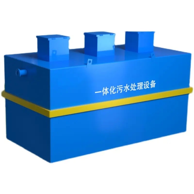
Establishing a comprehensive monitoring protocol requires understanding which parameters most directly impact reuse applications and manufacturing outcomes. Different semiconductor processes demand different water specifications, and treated wastewater quality varies depending on source streams and treatment technologies employed. Organizations must identify critical monitoring points, define acceptable thresholds for each parameter, and implement consistent testing procedures. This systematic approach prevents contamination risks, extends equipment lifespan, and maximizes the value extracted from wastewater treatment investments.
Critical Water Quality Parameters to Monitor
Conductivity and Total Dissolved Solids
Conductivity serves as a rapid indicator of total dissolved solids and ionic contaminants in treated semiconductor wastewater. High conductivity levels signal the presence of salts, minerals, and chemical residues that may interfere with semiconductor manufacturing processes or cause equipment corrosion and scaling. Monitoring conductivity provides early warning of treatment system failures or contamination events, allowing operators to adjust processes before reuse occurs. Industry standards typically specify maximum conductivity limits ranging from 500 to 2000 microsiemens per centimeter depending on the specific reuse application and semiconductor process requirements.
Total dissolved solids must be tracked alongside conductivity measurements to provide a complete picture of water composition. While conductivity measures electrical properties, total dissolved solids quantifies the actual mass of dissolved substances, offering complementary information about treatment effectiveness. Semiconductor fabs often require ultra-pure water with conductivity below 50 microsiemens per centimeter for certain process steps, necessitating continuous monitoring and potentially additional polishing treatment before reuse in critical applications.
pH and Chemical Balance
The pH level of treated semiconductor wastewater directly affects corrosion rates in distribution systems and process equipment compatibility. Acidic or alkaline water can damage pipes, cause scaling, or interfere with chemical reactions in manufacturing processes. Typical monitoring ranges maintain pH between 6.5 and 8.5 for most reuse applications, though specific semiconductor processes may require narrower bands. Regular pH monitoring prevents damage to infrastructure and ensures that reclaimed water does not introduce unwanted chemical reactions during manufacturing operations.
Chemical balance extends beyond pH to include specific ionic species that may have accumulated during wastewater generation. Semiconductor operations produce residues containing fluorine, phosphorus, nitrogen compounds, and various metals that treatment systems must remove or neutralize. Monitoring for these specific chemical constituents ensures treatment effectiveness and verifies that residual concentrations remain below levels that would compromise product quality or equipment performance during reuse cycles.
Particulate Matter and Microbial Contamination Screening
Suspended Solids and Turbidity Assessment
Suspended solids and turbidity in treated semiconductor wastewater can damage process equipment, clog cooling system channels, and introduce defects into product manufacturing. Monitoring turbidity through optical measurement provides rapid feedback on treatment system performance and identifies breakthrough events when contaminants bypass filtration stages. Most semiconductor reuse applications require turbidity below 0.5 nephelometric turbidity units to prevent fouling and maintain system reliability. Regular turbidity testing combined with visual inspection helps operators identify filter degradation or treatment inconsistencies before significant water quality degradation occurs.
Particle size distribution becomes particularly important when treated semiconductor wastewater feeds ultra-pure water systems or high-precision cooling loops. Even sub-micron particles can accumulate in heat exchangers or precision nozzles, reducing equipment efficiency and requiring costly maintenance. Advanced monitoring using laser particle counters enables detection of particles in the 0.5 to 100 micrometer range, ensuring that reclaimed water meets the stringent cleanliness requirements of semiconductor manufacturing. Implementing multi-stage filtration with appropriate monitoring between stages optimizes treatment effectiveness and water quality consistency.
Microbial and Biological Activity
Biological growth in treated semiconductor wastewater storage systems and distribution networks poses serious risks to reuse applications. Bacteria, algae, and biofilm formation can degrade water quality, produce odors, and introduce living contaminants into manufacturing processes. Regular microbiological testing including heterotrophic plate counts and ATP bioluminescence measurements quantifies biological activity and guides biocide treatment decisions. Semiconductor facilities typically maintain treated wastewater in cool, dark storage conditions and use preventive biocides to suppress microbial populations and maintain water integrity over extended storage periods.
Monitoring biofilm development inside recirculation pipes and cooling system channels requires periodic system inspections and preventive cleaning protocols. Even treated semiconductor wastewater contains residual organic compounds that can support limited microbial growth under favorable conditions, making proactive biological monitoring essential for maintaining water quality throughout the reuse system. Integrating ultraviolet treatment or supplemental chlorination into the reclaimed water circuit provides additional microbiological control and extends the time between system maintenance interventions.
Heavy Metal Content and Trace Contaminant Detection
Metal Ion Analysis and Trace Element Monitoring
Semiconductor manufacturing generates wastewater containing various metal ions including copper, tin, lead, nickel, and other trace elements that must be removed or reduced to safe reuse levels. Heavy metal monitoring through inductively coupled plasma mass spectrometry identifies concentrations of these elements and verifies that treatment processes achieve required removal efficiency. Different semiconductor processes generate different metal profiles, and treated wastewater quality specifications must align with the specific reuse application and regulatory requirements governing water reclamation in your facility or region.
Establishing baseline metal concentration profiles for your semiconductor wastewater helps identify treatment system degradation or process changes that might affect reuse safety. Monthly or quarterly comprehensive metal analysis combined with more frequent rapid screening methods ensures consistent compliance with water quality standards. Some metal ions can migrate or precipitate over time in storage, making periodic testing of stored reclaimed water important for confirming ongoing quality and identifying potential sludge formation or settling issues that might affect system performance.
Organic Compound Residuals and Process Chemical Traces
Organic residues from cleaning solutions, photoresists, and process chemicals remain in semiconductor wastewater even after primary treatment steps. Total organic carbon testing quantifies the remaining organic load and indicates whether additional activated carbon polishing or advanced oxidation processes are needed before reuse. Certain organic compounds can degrade seals, interfere with manufacturing chemistry, or leave deposits in critical equipment requiring separate monitoring and treatment protocols. Understanding your specific semiconductor process wastewater composition guides targeted treatment selection and establishes realistic reuse quality parameters.
Specific organic contaminants may require specialized testing methods beyond standard total organic carbon measurement, particularly if your treated semiconductor wastewater will be reused in ultra-pure water systems or semiconductor process steps sensitive to organic contamination. Gas chromatography or high-performance liquid chromatography analysis identifies individual organic species and their concentrations, enabling treatment process optimization and verification that reclaimed water meets application-specific purity requirements. Building a predictive model of how different treatment technologies affect your particular organic contaminant profile improves reuse system efficiency and water quality consistency over time.
FAQ
How frequently should water quality testing occur before semiconductor wastewater reuse?
Testing frequency depends on reuse application criticality, treatment system complexity, and regulatory requirements. Most facilities conduct daily or weekly conductivity and turbidity screening, monthly comprehensive water quality analysis, and quarterly metal content assessment. Microbial testing should occur monthly during normal operation with increased frequency if system upsets or contamination events are suspected. Starting with intensive baseline testing for 90 days helps establish normal parameter ranges and identify appropriate monitoring intervals for your specific operation.
What happens if treated semiconductor wastewater exceeds acceptable reuse quality parameters?
Exceeding quality limits requires immediate corrective action ranging from treatment system adjustment to temporary reuse suspension depending on which parameters fail. Minor conductivity or pH excursions often respond to treatment process optimization without significant delays. More serious issues like heavy metal breakthrough or microbial contamination may require emergency filtration, activated carbon treatment, or system flushing before resuming reuse operations. Establishing clear escalation procedures and having backup treatment capacity ensures flexibility to address quality incidents while minimizing production disruptions and water disposal costs.
Can treated semiconductor wastewater be used for all manufacturing processes after quality verification?
Different semiconductor manufacturing steps have varying water purity requirements, so not all treated reclaimed water can be reused for all applications. Cooling water and cleaning processes generally tolerate lower purity levels, while ultra-pure water applications and certain chemical processes demand substantially higher quality. Develop a quality tiering system that matches treated semiconductor wastewater specifications to appropriate reuse applications, potentially combining intermediate-quality reclaimed water for lower-demand uses with further-polished water for critical manufacturing steps. This approach maximizes reuse value while preventing quality-application mismatches that could compromise product integrity or equipment reliability.

 EN